The original Central Data board uses 3624 PROMs. On the PHCC-board those are replaced by Philips/Signetics 82S115 PROMs. The chips are similar, but have different chip select signals.
- The 3624 has four Chip Enable signals: CE1
•, CE2•, CE3 and CE4. CE1•and CE2•are active low, C3 and CE4 are active high. - The 82S115 has CE1
•(active low) and CE2 (active high), and also FE1, FE2. During normal operations fusing pins FE1 and FE2 may be grounded or left floating. - The 82S115 also has a Strobe input. If Strobe is held high, the device functions in a manner identical to conventional bipolar ROMs.
I have five 82S115 PROMs (see the description of Popmon). One of them is missing, and one of the remaining chips developed bad bits: some 0’s have spontaneously flipped to 1’s. Apparently PROMs degrade over time!
The nicest solution from a restoration perspective would be to source new chips. I do not have a suitable programmer, and instead I looked at an alternative that was both more flexible and cheaper.

The ATMEL AT28C64B (full documentation) is an 8 Kbyte EEPROM. During normal read operations it behaves just like a static ROM chip, but it can also be programmed simply by writing to an address location. There are some limitations to writing: at most 64 bytes can be written in a single operation, and after that operation the chip must be given a few milliseconds to program the bytes. It cannot be used as a non-volatile static RAM chip, but nearly so. For example, changing a single byte can simply be done using the Alter Memory command in the monitor program. And it uses only a single 5 Volt supply voltage. My local electronics shop sells the AT28C64B for less than €12.
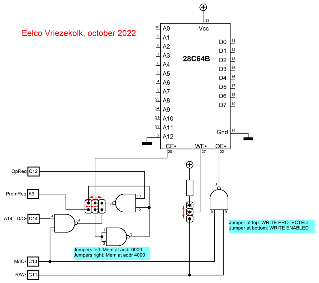
On the daughterboard I added the following simple circuit. The connectors on the left refer to the P1 bus. Note that the PHCC-board has room for eight PROMs, for a total of 4 KByte. The AT28C64B is twice that size, and therefore the top address line is unused and connected to ground. Signals marked with a bullet • are active-low; normally active-low is indicated by an overline, but that is cumbersome in sPlan.

The first jumper allows you enable/disable the write function. During normal operations it is safer to disable the WE• signal.
The second jumper allows you to position the memory at address 0000 or 4000. During normal operations the chip replaces the PROMs on the board: the location will be set to 0000. But for initial programming it is useful to use the original monitor program to boot the computer, load a small utility program, and flash the chip to its desired contents.
Note that PromReq is a combination of A12, A13, A14 (all low) and OpReq (high). PromReq is active high.
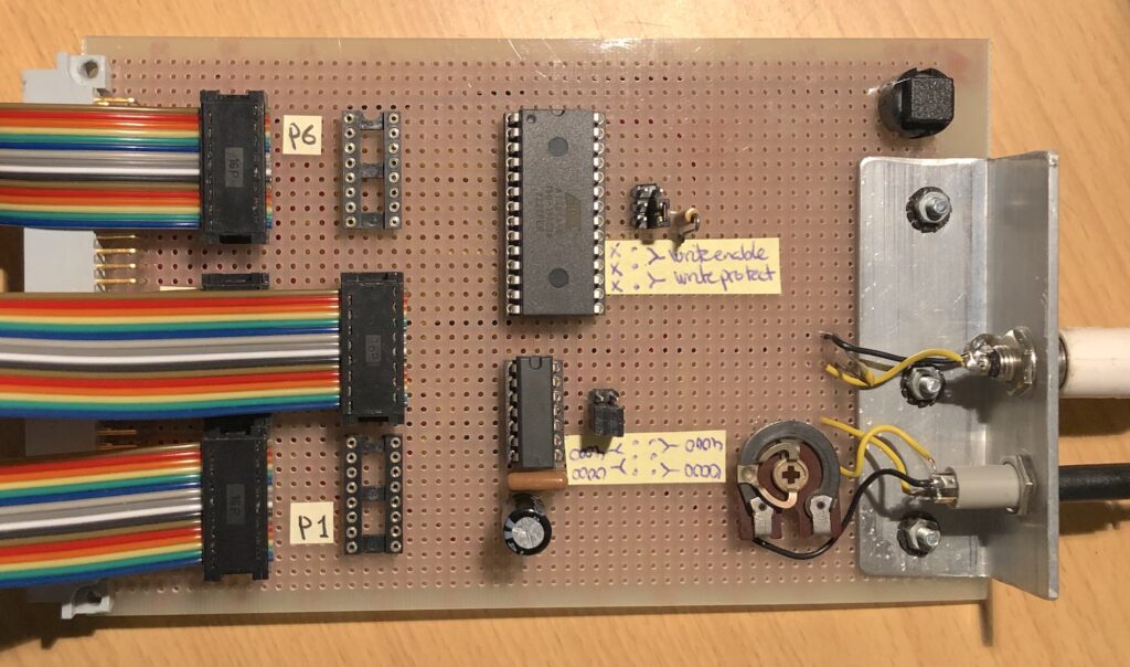
The photo above shows the circuit as built on the daughterboard. The ribbon cables connect to the main computer board. The AT28C64B and 74LS00 in their sockets in the middle. On the right a black reset button and a frame for audio and video output. Audio connects to my Macbook, that acts as a cassette recorder.
The following utility program can be used to flash the AT28C64B chip. Note that one way to check that the chip has completed its write operation is to re-read the last byte written. As long as re-reading yields a different value than was written, the chip is still busy.
                                dflt    16
                                org     1510

1510                    MEMPROG:
1510: 1B 06                     bctr,un Mprog

1512                    FROM:
1512: 00 00                     ACON    0000
1514                    TO:
1514: 0C 00                     ACON    0C00
1516                    FLASH:
1516: 40 00                     ACON    4000


1518                    Mprog:
1518: 08 78                     lodr,r0 FROM
151A: CC 15 D7                  stra,r0 PFROM
151D: 08 74                     lodr,r0 FROM+1
151F: CC 15 D8                  stra,r0 PFROM+1
1522: 08 72                     lodr,r0 FLASH
1524: CC 15 D9                  stra,r0 PTO
1527: 08 6E                     lodr,r0 FLASH+1
1529: CC 15 DA                  stra,r0 PTO+1

152C                    NextBlock:
                        ; Calculate the #bytes to program: TO-PFROM
152C: 77 09                     PPSL    WC+CAR
152E: 08 65                     lodr,r0 TO+1
1530: AC 15 D8                  suba,r0 PFROM+1
1533: C2                        strz,r2
1534: 08 5E                     lodr,r0 TO
1536: AC 15 D7                  suba,r0 PFROM
1539: C1                        strz,r1
153A: 75 08                     CPSL    WC
                        ; R1,R2 now contain the number of bytes to program
153C: 01                        lodz,r1
153D: 98 09                     bcfr,z  Maxblock
153F: E6 00                     comi,r2 0
1541: 1C 00 83                  bcta,eq RETU
1544: E6 40                     comi,r2 d'64'
1546: 99 02                     bcfr,gt GoProgram
1548                    MaxBlock:
1548: 06 40                     lodi,r2 d'64'

154A                    GoProgram:
154A: CA 36                     strr,r2 PLen
154C: 3F 15 B8                  bsta,un PROGRAM
154F: E7 FF                     comi,r3 h'ff'
1551: 98 06                     bcfr,eq IncAddrs
1553: 3F 15 96                  bsta,un ProgError
1556: 1F 00 83                  bcta,un RETU
1559                    IncAddrs:
1559: 77 08                     PPSL    WC
155B: 75 01                     CPSL    CAR
155D: 08 23                     lodr,r0 PLen
155F: 8C 15 D8                  adda,r0 PFrom+1
1562: CC 15 D8                  stra,r0 PFrom+1
1565: 20                        eorz,r0
1566: 8C 15 D7                  adda,r0 PFrom
1569: CC 15 D7                  stra,r0 PFrom
156C: 75 01                     CPSL    CAR
156E: 08 12                     lodr,r0 PLen
1570: 8C 15 DA                  adda,r0 PTo+1
1573: CC 15 DA                  stra,r0 PTo+1
1576: 20                        eorz,r0
1577: 8C 15 D9                  adda,r0 PTo
157A: CC 15 D9                  stra,r0 PTo
157D: 75 08                     CPSL    WC
157F: 1F 15 2C                  bcta,un NextBlock

1582                    Plen:
1582: 00                        DB      0


1583                    Msg:
1583: 45 72 72 6F 72 20         DB      "Error at block \00"
1589: 61 74 20 62 6C 6F
158F: 63 6B 20 5C 30 30
1595                    MSgC:
1595: 00                        DB      0
1596                    ProgError:
1596: 05 00                     lodi,r1 0
1598                    Ploop:
1598: 0D 75 83                  loda,r0 Msg,r1
159B: 18 0B                     bctr,z  Paddr
159D: C9 76                     strr,r1 MsgC
159F: C3                        strz,r3
15A0: 3F 03 96                  bsta,un WCHR
15A3: 09 70                     lodr,r1 MsgC
15A5: D9 71                     birr,r1 PLoop
15A7: 17                        retc,un
15A8                    Paddr:
15A8: 0E 15 D7                  loda,r2 PFROM
15AB: 3F 00 6A                  bsta,un HXOT
15AE: 0E 15 D8                  loda,r2 PFROM+1
15B1: 3F 00 6A                  bsta,un HXOT
15B4: 3F 00 24                  bsta,un LFCR
15B7: 17                        retc,un

                        ; Subroutine PROGRAM: Copy a block of bytes into Flash
                        ; In:
                        ;  R2: number of bytes to copy (max 64)
                        ;  FROM: address containing the data
                        ;  TO: address of the Flash memory
                        ; Return:
                        ;  r3: contains FF on error, any other number on success
                        ;
15B8                    PROGRAM:
15B8: A6 01                     subi,r2 1
15BA: 05 FF                     lodi,r1 h'ff'
15BC: 20                        eorz,r0
15BD: C3                        strz,r3            Counter
15BE                    LOOP:
15BE: 0D B5 D7                  loda,r0 *PFROM,r1,+
15C1: CD F5 D9                  stra,r0 *PTO,r1
15C4: 01                        lodz,r1
15C5: E2                        comz,r2
15C6: 98 76                     bcfr,eq LOOP

                        ; All written. Now compare the last byte written
15C8                    wait:
15C8: 0D F5 D7                  loda,r0 *PFROM,r1
15CB: ED F5 D9                  coma,r0 *PTO,r1
15CE: 18 06                     bctr,eq Done
                        ; Not yet ready, increment the counter
15D0: 87 01                     addi,r3 1
15D2: E7 FF                     comi,r3 h'ff'
15D4: 98 72                     bcfr,eq wait
15D6                    Done:
15D6: 17                        retc,un


15D7                    PFROM:
15D7: 00 00                     dw      0
15D9                    PTO:
15D9: 00 00                     dw      0

                        HXOT    EQU     006a
                        LFCR    EQU     0024
                        RETU    EQU     0083
                        WCHR    EQU     0396